|
Product Information
New Product Highlights

Device List/Description
Selection Guide
Technical Information
Application & Support
Obsolete Devices
& Suggested Replacements
Technical FAQs
Package Information
In the News
|
|
Power Control Products
Technical FAQs

What is power switching IC?
Power switching circuitry is required to complete the interface between electrical control signals (”C) and the loads.
The real-world function of a load may be in the form of motion, light, or sound. Depending on the complexity of the
control system, the interface circuit may be required to control a simple action to providing feedback signals and/or fault isolation.
What are Power+™ ICs?
Power+ ICs are monolithic power DMOS devices that feature multiple integrated transistors in surface-mount packaging.
These devices may include on-board control logic, limiting current, ESD protection, snubber circuitry, diagnostics,
and fault detection. Due to the high level of integration, Power+ ICs maintain significant cost advantage
(such as reduced component count and board-space along with minimized procurement and inventory expenses)
over discretes on a per-transistor basis.
What are some target loads/end-equipments/segments?
Power+ devices offer superior alternatives to discrete power MOSFETs and hybrids in many power switching
applications including driving fractional horsepower motors, solenoids, valves, relays, LEDs, and lamps.
Target segments are:
- EDP: printers, plotters, copiers, scanners, fax machines, power distribution switching.
With their low-on resistance and minimized power dissipation, these Power+ devices operate reliably in confined spaces.
Their surface-mount packaging is well-suited for modules with limited headroom.
- Industial: automated test equipment, process control systems, programmable machine tools, robotics,
instrumentation panels, person appliances, telecom line cards, moving signs, electronic games.
The ruggedness of the Power+ devices make them very attractive for industrial stringent environments.
They offer power handling capabilities, extended temperature ranges, and avalanche energy absorption.
- Automotive: powertrain (engine, transmission, and emission controls), body and chassis,
instrumentation, passive restraints, anti-lock brake systems, electronic fuel injectors, tell-tale lights.
For this cost-conscious segment and its extremely harsh operating environment, Power+ devices offer
wide operating ranges, high level of integration, short cycle time to market, and cost-effectiveness.
These are low-cost and low-risk catalog alternatives over custom solutions.
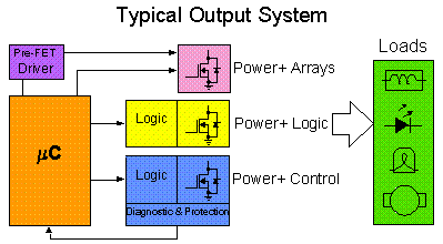
What are the different families in Power+ product line?
TI offers three families of Power+ devices, each offering a different level of integration
depending on systems requirement and price sensitivity.
- Power+ Logic™ - features high speed CMOS control logic integrated with
multiple power DMOS FETs. These are 8-channel devices with various CMOS control logic including
addressable latch, D-type latch, and shift register.
- Power+ Control - features integrated power ICs with diagnostic and protection
functions including FET predrivers with companion Power+ Array drivers.
- Power+ Arrays™ - features integrated rugged power DMOS FETs in configurations
such as 3-phase H-bridge and common-source.
Why is the TPIC6Axxx not pin-for-pin compatible with the other Power+ Logic™
devices (TPIC6xxx or TPIC6Bxxx)?
The output current of the 6Axxx is 350mA per channel versus 150/250mA per channel for
the 6xxx/6Bxxx, respectively. Layout of the 6Axxx was focused around optimizing thermal
performance due to increased current capability and, as a result, the layout was not
pin-for-pin compatible with the 6xxx and 6Bxxx devices.
Are there any layout precautions with the Power+ Logic devices to minimize parasitic
inductance/noise/crosstalk?
When designing with Power+ Logic devices, always use a bypass capacitor between Vcc and
logic supply ground. We suggest a 0.1”F ceramic capacitor for this function.
Also, route the ground for the logic interface circuits separately from the power ground bus.
Make only one tie between the two and place this tie near the pin connected to the logic ground.
Finally, use short, sizeable traces to minimize voltage drops across the layout.
|