TLC5628C and TLC5628I are octal 8-bit digital-to-analog converters (DACs). The operation and features are similar to the TLC5620 quad DAC. This device has two buffered reference voltage inputs, each reference feeds four DACs. Each DAC output voltage range can be programmed to one or two times the reference. Each DAC is programmed with a 12-bit word using a three wire serial interface. The digital registers are double buffered to allow simultaneous update of all DACs. Typical applications include: digitally controlled amplifiers/attenuators, mobile communications, automatic test equipment, process control and signal synthesis.
This device is available in 16-pin small outline (D) and 16-pin plastic dip (N) packages. The TLC5628C is characterized for operation from 0° C to 70° C. The TLC5628I is characterized for operation from -40° C to 70° C.
The TLC5620C and TLC5620I are quad 8-bit digital-to-analog converters (DACs). Each DAC has a separate buffered reference input. Each DAC can be programmed for an output of one or two times the reference voltage. Digital input and control is via a three wire CMOS compatible serial bus. The device operates on a single supply of 5 V. The digital interface uses an eleven-bit word to communicate address, data and mode for each DAC. The DAC registers are double buffered allowing all DACs to be updated simultaneously. The serial interface operates at clock frequencies up to 1 MHz. Multiple DACs and a serial interface make this device suitable for applications such as: digitally controlled amplifiers/attenuators, mobile communications, automatic test equipment, process control and signal synthesis.
This device is available in 14-pin small outline (D) and 14-pin plastic dip (N) packages. The TLC5620C is characterized for operation from 0° C to 70° C. The TLC560I is characterized for operation from -40° C to 70° C.
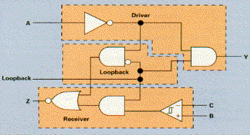
The SN75LBC786 combines four RS-423-B drivers/receivers with loopback circuits to provide fast data transmission, with hands-off testing of the drivers/receivers and partial testing of the lines. Driver slew rates are controlled with only one resistor. The receivers are RS-232 compatible with the addition of external resistors to meet the RS-232 input resistance specification of 3 kOhms to 7 kOhms. Both the drivers and receivers can handle voltages up to ± 25 V under normal operation. During normal operation, the device functions as four independent RS-423-B driver/receiver pairs. In loopback mode, the device electrically isolates itself from the outside world and loops the output of the drivers back into the receivers to check device functionality. The fully EIA/TIA-423-B compatible device will support nominal data rates of 120 KBPS and cable lengths up to 1.2 km.
The SN75LBC786 is characterized for operation from 0° - 70° C. The device is available in the 28-pin wide body SOIC (DW) package.
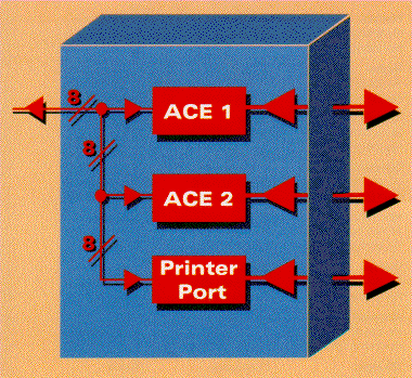
The TL16C552AI is the industrial version of the TL16C552A, which is an enhanced dual channel version of the TL16C552 asynchronous communications element (ACE). Each channel performs serial-to-parallel conversion on data received from peripheral devices or modems. Parallel-to-serial conversions occur on data characters transmitted by the CPU. The status information available to the CPU includes the type and condition of the performed operation and of any encountered error conditions. The TL16C552AI also provides the user with a fully bi-directional parallel Centronix printer interface port. The industrial temperature range is -40° C to 85° C.
TI has recently reduced the suggested resale price of the TLC5510NSLE to $5.00 (in 1 K quantities). This reduction will allow designers to upgrade to higher resolution and/or sampling rates at little or no extra cost. Targeted applications include Video Conferencing, QAM and QPSK Demodulators, Medical Imaging, low end Digital Oscilloscopes and a variety of video end equipments. The TLC5510NSLE is a high speed CMOS ADC that operates on single 5VDC supply, dissipates only 90 mW of power, has internal S/H, tri-state outputs and internal divider network to produce 2 V reference from VDDA.
The TL5632 is a low-power, high-speed, 3-channel, 8-bit digital-to-analog converter (DAC). This three channel DAC is designed to produce the RGB video output signal. The DAC operates from a single 5-V supply and typically consumes only 350 mW. The TL5632 provides an internal reference voltage generator for producing standard video output levels. This converter can operate from DC to 60 MHz making it suitable for use in digital television, computer video processing and high-speed data conversion. The TL5632 is characterized for operation from 0° to 70° C, and is available in a 44-pin plastic quad flatpack (FR) package.
The SN75185 is a bipolar RS-232 device combining three drivers and five receivers. The pin-out matches the flow-through design of the SN75C185 to decrease part count, reduce required board space, and allow easy interconnections. The 10 KV ESD protection increases reliability and eliminates the need for external protection components. Switching speeds of the SN75185 are high enough to support rates up to 120 KBPS with shorter cable lengths. The all-bipolar SN75185 provides a rugged low-cost solution for this function. The SN75185 is characterized for operation from 0° to 70° and is available in the 20-pin plastic dip of wide body SOIC (DW) package.
Vol 11, Spring, 1995