

The TLC5540 digitizes high bandwidth analog signals with 8 bit
resolution at a minimum conversion rate of 40 MSPS. This product
combines high speed with low power consumption and cost to create
a new price/performance point for high speed ADCs. Features include
an analog input bandwidth of 75 MHz (greater than Nyquist), internal
sample & hold, internal self bias reference network and three-state
outputs. Fabricated in a CMOS process, the TLC5540 requires a
single 5 V supply for operation and dissipates only 85 mW of power
typically at ![]() = 40 MSPS.
= 40 MSPS.
The wide analog input bandwidth allows this ADC to be used in undersampling applications to digitally transform an IF signal to baseband information and eliminate the costly analog down converter components. The TLC5540 implements a semi-flash architecture to allow the combination of wide analog input bandwidth, high speed and low power. The low analog input capacitance of 4 pF (typ.) eases the drive requirements of the interface circuits.
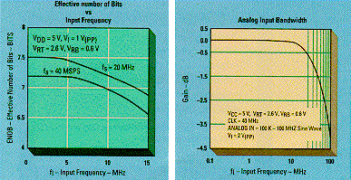
The TLC5540 is also an excellent choice for traditional Nyquist based digital signal processing applications. Specified with both static and dynamic characteristics, the TLC5540 delivers 7.6 effective bits with sampling rate of 20 MSPS and 7.0 effective bits with 40 MSPS. Differential Non-Linearity is specified at ± 0.75 LSB and Integral Non-Linearity at ±1.0 LSB. Spurious free dynamic range (SFDR) is typically 46 dBc at 20 MSPS and 42 dBc at 40 MSPS. This device is available in a 24 pin SOIC package.
Vol 16, April, 1996