TLC8188 10-bit 4 MSPS
CIS/Linear CCD Sensor Processor
[Features] [Applications]
[Functional Description] [Documentation]
Features:
- 0 to 2.5V programmable input offset correction range with 8-bit resolution. This is optimal performance for CIS scanners, and allows full use of ADC's dynamic range.
- Auto-cycling inputs, PGA gain and offset for each color; each color has its own register. This simplifies design of host control.
- Internal reference voltages reduce component count and improves system accuracy.
- Supports CIS interface as a low-cost scanning option.
- Supports both CIS and CCD sensors for the option of using the device across multiple platforms, reducing inventory costs.
- Low-cost linear CCD interface with support for both single output and RGB parallel output CCDs
- Configure internal registers through either parallel or serial interface ports; read back register values through serial port. This provides a flexible host interface.
RETURN TO TOP
Applications:
Fully integrated analog processing circuitry and low-cost make the TLC8188 an ideal sensor interface solution for imaging applications such as sheet-fed and flatbed scanners, multifunction products that combine copier, fax and scanner functions, digital copiers, bar code readers and fingerprint scanners.
RETURN TO TOP
Functional Description:
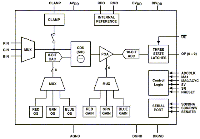
 Texas Instruments' TLC8188 is a highly-integrated, single-chip analog signal processor/digitizer designed to interface to Contact Image Sensor (CIS) and linear Charge-Coupled Device (CCD) image sensors for scanner applications. The TLC8188 performs all analog processing functions necessary to maximize the dynamic range, correct various errors associated with the CIS and the linear CCD sensors, and then digitize the results with an on-chip analog-to-digital converter (ADC).
The TLC8188 is optimized for use with contact image sensors(CIS) and characterized by its ability to eliminate the large offset in the CIS output signal. A digital-to-analog converter (DAC) can be programmed to generate 0 to 2.5V (±0.5V in CCD mode) offset calibration range with 8-bit resolution. The offset is subtracted before the gain stage to maximize dynamic range.
The device includes an auto-cycling feature to automatically sequence the analog inputs, PGA gain, and offset for each color, thus simplifying the design of the host ASIC control. The gain and offset may also be specified by external control pins or by internal setup registers without auto-cycling. In mono applications, input analog mux can be forced to a single color while the gain and offset registers are still auto-cycled, externally selected, or internally programmed.
The TLC8188 operates from a single 5V power supply and its digital interface is 3V compatible. The normal power consumption of the TLC8188 is 190mW and it consumes just 35mW in power-down mode.
RETURN TO TOP
Documentation:
View the TLC8188 datasheet
RETURN TO TOP
|