Single TI CMOS ASIC Provides 622 Mbps Interfaces and 20 Gbps Throughput in High Speed Telecommunications
 DALLAS (Jan. 26, 1998) - A CMOS ASIC (Application Specific Integrated Circuit) utilizing multiple 622 megabits-per-second (Mbps) interfaces and achieving 20 gigabits-per-second (Gbps) bandwidth was announced today by Texas Instruments (TI) and is shipping in volume. The ASIC
device replaces expensive BiCMOS chips and is working in production telecommunications equipment that is expected to ship during the first quarter of 1998. Using advanced CMOS 622 Mbps interfaces, TI's TGC4000 ASIC product allows designers of high-speed telecommunications and networking systems to reduce overall system costs, size and power consumption.
DALLAS (Jan. 26, 1998) - A CMOS ASIC (Application Specific Integrated Circuit) utilizing multiple 622 megabits-per-second (Mbps) interfaces and achieving 20 gigabits-per-second (Gbps) bandwidth was announced today by Texas Instruments (TI) and is shipping in volume. The ASIC
device replaces expensive BiCMOS chips and is working in production telecommunications equipment that is expected to ship during the first quarter of 1998. Using advanced CMOS 622 Mbps interfaces, TI's TGC4000 ASIC product allows designers of high-speed telecommunications and networking systems to reduce overall system costs, size and power consumption.
The total throughput of 20 Gbps is achieved in this TGC4000 application with 64 signals (32 inputs and 32 outputs), each communicating at a speed of 622 Mbps. The 0.35-micron gate array design contains 1.4
million transistors and forms the heart of an OC-192 public telecommunications system.
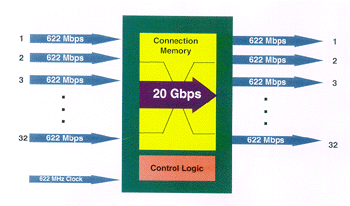
622 Mbps I/0s enable Texas Instruments TGC4000 ASIC to achieve 20 Gbps throughput
The key to the device's throughput capability lies in a high-performance Current Mode Logic (CML) interface which has been designed to operate at more than 850 Mbps. Other high-speed interfaces are also supported in this technology, including 850 Mbps Emitter Coupled Logic (ECL) type and 622 Mbps Low Voltage Differential Swing (LVDS). Supporting functions such as clock recovery and bit phase aligners are also available. Integrating these high-performance interfaces eliminates the need for power-hungry and expensive gallium arsenide (GaAs), Bipolar, or BiCMOS devices that have historically been required for high-speed interface applications. This integration capability also simplifies board design, resulting in significantly lower system development costs.
"By working closely with the customer, we were able to achieve first-pass design success," said Shinichiro Yamazaki, ASIC Telecommunications Business Unit Manager at TI. "The well-established 0.35 micron process makes the TGC4000 solution a very cost-effective one. As we migrate designs to our advanced 0.18-micron technology, we will see even greater improvements in speed, density and power
consumption, resulting in a significant reduction in the number of chips required on a board."
TGC6000 PRODUCT WILL PROVIDE 80 GBPS THROUGHPUT
TI offers even higher performance in its latest 0.18-micron TGC6000 ASIC product. Interfaces capable of speeds up to 2.5 Gbps will be supported, potentially quadrupling the throughput to over 80 Gbps, while dissipating very low power and providing multiple high-speed channels integrated on one ASIC. The smaller size and higher speed of TI's 0.18-micron technology will save system costs by further reducing the number of chips required in a high-speed telecommunications or networking system. Power consumption will also drop at the 0.18-micron technology node by at least 70 percent in the core leading to chip power dissipation savings of greater than 50 percent.
The high-speed interfaces and supporting circuitry are proving to be essential in high-performance Synchronous Optical Network (SONET) and Synchronous Digital Hierarchy (SDH) telecommunication systems as well as in networking Gigabit Ethernet or Internet Protocol (IP) systems.
Availability
TI is offering designers a TGC4000 test chip and test board to evaluate these high-speed interfaces and macros in their system designs. The TGC4000 product has been available since 1996. TI has accepted
design engagements and is currently executing designs using the TGC6000 (0.18-micron) technology. Additional design engagements in both technologies are available now.
For more information about TI's ASIC products, please visit  http://www.ti.com/sc/docs/asic/prodinfo.htm http://www.ti.com/sc/docs/asic/prodinfo.htm
# # #
|