
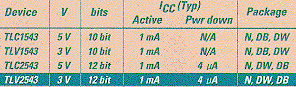
The TLV2543 operates at 3.3 V, consumes only 1 mA typical, 2.5 mA (max) while delivering a 12-bit resolution at 66 ksps throughput. A software programmable power down mode reduces power consumption to 4 µA typical, 25 µA (max). A built-in multiplexer provides 11 single-ended analog input channels plus three internal test modes. The TLV2543 includes an onboard conversion clock. Its generic interface provides an easy interface to virtually all types of processors equipped with a 3-wire SPI compatible serial interface. It provides a low system cost for a 12-bit data acquisition system.
The TLV2543 also maximizes the design/manufacturing flexibility with the same pinout as the 5 V TLC2543. Therefore, systems can be easily upgraded from an existing 10-bit design using the TLV1543. Manufacturers will be able to build a family of products with different price-performance characteristics based on a single design.
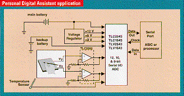
Battery powered process monitors and testers can be implemented with this low cost high performance ADC to achieve longer battery life. Next generation cellular phones and PDAs that require higher quality pen digitizer interface can benefit from the small SSOP package and multiple input channels available for temperature, battery voltage, panel brightness and other system variable management. Other applications include pixel conversion in color printers, offset adjust in instrumentation and data logging.
TLV2543 is available in 20-pin DIP, SO and SSOP packages.
Vol 14, December, 1995
 Return to Showcase Home Page