|
|
Special Focus on Logic Breaking the high-speed barrier LVC logic now specified to 1.8 V New bus switch keeps data moving LV CMOS redesigns provide faster speeds, lower power and lower noise New UBT optimized for high-performance backplane uses Industry cross-reference to TI low-voltage logic
|
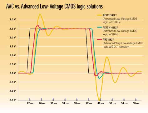
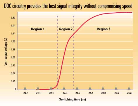
Breaking the high-speed barrier As the industry’s first logic devices to achieve propagation delays of less than 2 ns maximum at 2.5 V, the new AVC (Advanced Very-low-voltage CMOS) logic family from Texas Instruments will give designers the tools to create tomorrow’s advanced high-speed systems. Although optimized for 2.5-V systems, AVC logic supports mixed-voltage systems, providing compatibility with and operation at 3.3 V and 1.8 V. The AVC family features TI’s revolutionary new Dynamic Output Control (DOC™) circuitry that automatically lowers the output impedance of the circuit during a signal transition and subsequently raises the impedance after signal transmission to reduce noise. Trends in advanced digital electronics design continue to emphasize lower power consumption, lower supply voltages, faster operating speeds, smaller timing budgets and heavier loads. Many designs are making the transition from 3.3 V to 2.5 V, and bus frequencies are increasing beyond 100 MHz. However, signal integrity should not be compromised in an effort to meet all of these design parameters. The new AVC family is designed to meet the needs of these systems, including next-generation high-performance workstations, PCs, networking servers and telecommunications switching equipment. The quest for speed Traditionally, designers seeking fast speeds had to make tradeoffs with signal integrity. TI’s AVC family is the industry’s first to provide both extremely low propagation delays and high signal integrity. As supply voltage levels decrease, so do digital signal transition swings. The shorter the voltage swing from a recognized "high" to a recognized "low" (or vice versa), the more quickly a device can make such a signal transition. In this way, lower voltage standards pave the way for increasing speeds. However, even with reduced voltage swings increasing speeds have always meant increasing noise levels. As a rule of thumb, the faster a device makes a digital signal transition, the more signal overshoot or undershoot will be encountered. So, signal integrity was traditionally compromised for faster speeds. Designers typically used external resistors on output circuitry to keep noise levels under control, but this meant additional cost and board space requirements. Suppliers began offering high-speed logic solutions with Series Damping Resistors internal to the device’s output circuitry. This eliminated the need for external resistors (and the added cost and board space), but using these Series Damping Resistors did mean paying a speed penalty. Until now, families like ALVC (Advanced Low-Voltage CMOS) that were available with Series Damping Resistor options were the best solutions available for optimizing speed without compromising signal integrity. TI’s AVC family with DOC ends the need for compromise. DOC circuitry lowers output impedance during signal transition to drive the load. Subsequently, when the transition passes through the threshold voltage, DOC raises the output impedance to reduce noisy signal overshoots and undershoots. In this way, AVC only uses high drive when it is needed—during the heart of a signal transition. Power consumption The drive for lower power consumption is one of the most pervasive trends in advanced digital electronics. It is especially important to increase the life of battery-powered portable equipment. Reduced heat dissipation from lower power consumption simplifies heat removal and decreases the amount of packaging area needed. This in turn leads to smaller and less expensive products. Another effective way to reduce power dissipation is to decrease the operating voltage. The AVC family was designed to operate at 2.5-V supply voltage to enable high-performance, low-power advanced designs. Not simply a scaled-down 3.3-V LVTTL family, the devices were conceived and designed for optimized performance at 2.5 V. Advanced design features Some of the advanced features of the AVC family include:
|