|
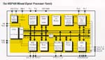
Product Information MSP430x11x Product Information Device List/Description and Peripheral Overview Development Tools
Technical Information |

[MSP430x310 Devices] [MSP430x320 Devices] [MSP430x330 Devices] [
The 16-bit RISC CPU core is a highly orthogonal structure that offers much more than the standard 4- and 8-bit microcontrollers. Every instruction can be used with each of the seven different addressing
modes. Also, the reduced instruction set of 51 instructions contains only basic 27 core instructions.
Low Power Modes
Power consumption with active peripherals is 400uA, but one of the advantages of the MSP430 devices is the user-selectable power-down modes. The user can switch off the unnecessary peripherals by simply setting bits in a control register. For example, the system can operate from the 32kHz clock instead of 3.3 MHz with the timers and LCD still active. The wake-up can be initiated by the timer or from an external interrupt.
Oscillator/FLL Module
The oscillator module generates the MCLK system clock with 3.3 MHz from an externally connected 32kHz crystal. The Digital Controlled Oscillator (DCO) starts operation immediately after a reset or interrupt occurs, providing a working system in a fraction of the time needed with conventional microcontrollers.
The A/D converter offers six inputs to convert analog signals in a 14-bit digital value over the full supply voltage range, or a 12-bit resolution in each of four separate ranges. The integrated current source can be programmed with an external resistor to connect current driven sensors.
The Timer/Port module can perform resistive to digital conversion by measuring the charge/discharge time of an external capacitor. If this function is not needed, the module can be used as a 16-bit timer. The watchdog timer can be used in 15-bit watchdog mode or in 16 bit general purpose timer mode. The Basic Timer includes two 8bit timers for general use. It generates the basic LCD frequency and supports the real time clock function.
The LCD module can drive up to 120 segments in 1 - 4 MUX mode. The I/O ports can be individually configured and handles the interrupts on every port-pin. The 8-bit Timer/Counter supports serial
communication protocols on the I/O port.
The H/W multiplier module performs 16x16, 16x8, 8x16 and 8x8 multiplications. Just loading the operands into the multiplier makes the result available in a register. No extra cycle is needed for the
multiplication. This feature extends the MSP430 CPU's processing power.
The Timer_A module consists of a 16-bit timer/counter and five registers, which can be configured in capture or compare mode. The capture mode is mainly used to measure external or internal events, while the compare mode permits generation of pulse-width modulated (PWM) output signals for various purposes like D/A conversion or PWM.
The new USART module includes two functions for serial communication, a standard asynchronous communication protocol (UART up to 115.2 kBaud) and a serial peripheral interface (SPI). One bit in a control register defines the mode used. It is also possible to switch between the two modes in operation.
Notes:
|