InsideShowcase (Volume 23) is available in HTML and PDF format. - 319KB
|
ADCs enable single chip solution from CCD output to digital domainProduct Features
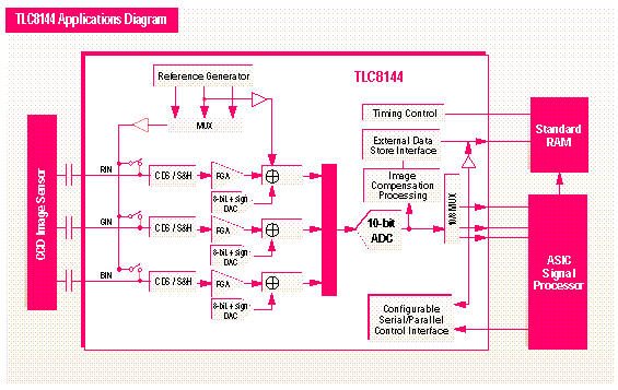
The TLC8044 and TLC8144 both feature separate RGB inputs, bipolar analog signal offset correction, and a 3-to-1 RGB analog MUX. In addition, the internal sample and hold circuitry allows them to handle both color and gray-scale operations. The TLC8044 features a fully differential analog signal path and has a 12-bit, 6-MSPS analog-to-digital converter that will support up to 36-bit color designs. The TLC8044 also affords the designer the option of using pixel-by-pixel digital correction circuitry, six internal offset correction registers (red, green, blue, even and odd pixels), and three internal registers to correct pixel shading. For global error correction, the TLC8044 offers both global offset and global gain adjustment for each color channel. The TLC8144 uses a single-ended analog signal path that includes 3 independent analog programmable gain amplifiers (PGA's) and a 10-bit 6-MSPS analog-to-digital converter that will support up to 30-bit color. The TLC8144 is able to perform pixel-by-pixel compensation of pixel response non-uniformity (PRNU) using data that is stored externally. Alternatively the designer has the option of bypassing this step. The output of the A/D can be passed directly to the controlling processor. This entire family of CCD interface devices features an easy interface to a host processor. The TLC8044 has a programmable output word length of 8,10,12, or 16 bits, a separate programmable threshold detect output for each color (for OCR operations), and a three wire serial input bus that sets all global and default correction values. The TLC8144 also incorporates interface flexibility. It features a flexible output architecture that allows the 10-bit output data to be accessed by either a 10-bit bus or via a time-multiplexed 8-bit bus. The TLC8144 is the internal sample and hold circuitry allows them to handle both color and gray-scale operations. The TLC8044 features a fully differential analog signal path and has a 12-bit, 6-MSPS analog-to-digital converter that will support up to 36-bit color. The TLC8044 also affords the designer the option of using pixel-by-pixel digital correction circuitry, six internal offset correction registers (red, green, blue, even and odd pixels), and three internal registers to correct pixel shading. For global error correction, the TLC8044 offers both global offset and global gain adjustment for each color channel. The TLC8144 uses a single-ended analog signal path that includes 3 independent analog programmable gain amplifiers (PGAs) and a 10-bit 6-MSPS analog-to-digital converter that will support up to 30-bit color. The TLC8144 is able to perform pixel-by-pixel compensation of pixel response non-uniformity (PRNU) using data that is stored externally. Alternatively the designer has the option of bypassing this step. The output of the A/D can be passed directly to the controlling processor. This entire family of CCD interface devices features an easy interface to a host processor. The TLC8044 has a programmable output word length of 8,10,12, or 16 bits, a separate programmable threshold detect output for each color (for OCR operations), and a three wire serial input bus that sets all global and default correction values. The TLC8144 also incorporates interface flexibility. It features a flexible output architecture that allows the 10-bit output data to be accessed by either a 10-bit bus or via a time-multiplexed 8-bit bus. The TLC8144 is programmed using a simple serial or an 8-bit parallel interface. Both only draw 400-mW of power from a single 5-V supply. The TLC8044 is available in a 64-pin mini-PQFP package (FN) and the TLC8144 is available in a 48-pin TQFP package (PT).
Vol 23 August, 1997 |