|
Showcase (Volume 28) is available in HTML and PDF format. - 351KB
|
TI's LVDS product portfolio continues to growProduct Features
Texas Instruments has established itself as the leader in Mixed-Signal and Analog products, and has 30 years of experience in the Data Transmission arena. TI's newest data transmission family, Low-Voltage Differential Signaling (LVDS), has recently increased its product portfolio to include guaranteed AC testing, quad drivers and receivers with enable, dual drivers and receivers, and a new Evaluation Module (EVM).
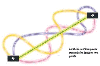
Compared to previous standards, TI's LVDS drivers and receivers offer speeds up to 400 Mbps, consume 1/8 the power of R5422, and radiate 1/10 the EMI of the best single-ended input/output (I/O). Designers who are presently using ECL and PECL technologies to attain speeds up to 400 Mbps will appreciate the ultra-low power of LVDS and the simplicity of its line termination, a single 100- TI's LVDS drivers and receivers meet or exceed the requirements of ANSI TIA/EIA-644. LVDS low-voltage swings of 350 mV (typical), 3.3-V supply voltage, and current-mode drivers lower power consumption. The power dissipation of a driver is 25 mW (typical) per driver at 200 MHz, while the power dissipation of a receiver is 60 mW (typical) at 200 MHz. In order to reach the high speeds of 400 Mbps, the driver has a typical output voltage rise and fall times of 750 ps. The driver's typical propagation delay time is 1.7 ns, while the receiver's typical propagation delay time is 1.4 ns. Both drivers and receivers are characterized for operation in industrial temperature, from –40°C to 85°C. TI recognizes the need for high ESD protection in the industry and therefore designed these products with a bus-terminal ESD protection which exceeds 8 kV. These products are offered in SOIC packaging. New Guaranteed AC Testing The previously released quad driver and receiver, SN65LVDS31 and SN65LVDS32, have been re-characterized to include minimum and maximum AC testing. The new revised data sheets show the minimum and maximum propagation delay time of the drivers as well as the receivers. The driver's propagation delay time has a minimum of 1 ns and a maximum of 2.5 ns. The receiver's propagation delay time has a minimum of 1.4 ns and a maximum of 4.1 ns. These characteristics also apply to the new LVDS products, SN65LVDS3486/87 and SN65LVDS9637/38. New Quad Driver and Receiver with Enable, SN65LVDS3487 and SN65LVDS3486 The new quad driver and receiver, SN65LVDS3487 and SN65LVDS3486, have enablers that allow the drivers and receivers to be turned on in pairs. This characteristic differentiates them from the previously released SN65LVDS31 and SN65LVDS32 which had to have all four drivers and receivers enabled at once. Designers will be able to choose the device which offers the most cost-effective solution to their application. The 'LVDS3487 and 'LVDS3486 follow the popular footprint of the MC3487 and MC3486. New Dual Driver and Receiver, SN65LVDS9638 and SN65LVDS9637 The new dual driver and receiver, the SN65LVDS9638 and SN65LVDS9637, respectively, broaden TI's LVDS products offerings. These devices have the same innovative characteristics as the quad drivers and receivers, with the only difference being the number of drivers and receivers per chip. The 'LVDS9638 and 'LVDS9637 follow the pin-configuration of µA9638 and µA9637, the industry's standard. New LVDS EVM
Vol 28 August, 1998 |
| TIA/EIA-644 Drivers and Receivers | |||||
| SN65LVDS31 |
|
|
|
|
|
| SN65LVDS32 |
|
|
|
|
|
| SN65LVDS3487 |
|
|
|
|
|
| SN65LVDS3486 |
|
|
|
|
|
| SN65LVDS9638 |
|
|
|
|
|
| SN65LVDS9637 |
|
|
|
|
|
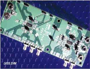 A new EVM which allows designers to evaluate TI's LVDS products is now available. This EVM will let designers play with different LVDS configurations. The EVM can be set up for point-to-point transmit-receive configurations, a multidrop configuration, and even receive some 422 data into an LVDS receiver. Other topologies can also be created such as parallel drivers for high current mode, multipoint schemes with multiple driver/receiver (pseudo 485) and much more.

